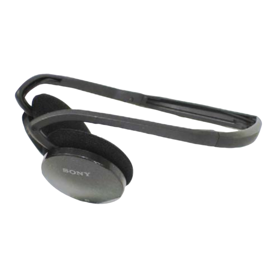
Sony DR-BT21G Service Manual
Wireless stereo headset
Hide thumbs
Also See for DR-BT21G:
- Operating instructions manual (80 pages) ,
- Instruction manual (88 pages) ,
- Specifications (21 pages)
Table of Contents
Advertisement
Quick Links
SERVICE MANUAL
Ver. 1.1 2007.06
General
Communication System
Bluetooth Specification version 2.0
Output
Bluetooth Specification Power Class 2
Maximum communication range
*1
Line of sight approx. 10 m (30 ft)
Frequency band
2.4 GHz band (2.4000 GHz – 2.4835 GHz)
Modulation method
FHSS
Compatible Bluetooth Profiles
A2DP (Advanced Audio Distribution Profile)
AVRCP (Audio Video Remote Control Profile)
HSP (Headset Profile)
HFP (Hands-free Profile)
Supported Codecs
*3
SBC
*4
, MP3
Transmission range (A2DP)
20 - 20,000 Hz (Sampling frequency 44.1KHz)
Supplied accessory
AC power adaptor (1)
Operating instruction (1)
*1
The actual range will vary depending on factors such as obstacles
between devices, magnetic fields around a microwave oven, static
electricity, reception sensitivity, aerial's performance, operating
system, software application, etc.
*2
Bluetooth standard profiles indicate the purpose of Bluetooth
communication between devices.
*3
Codec: Audio signal compression and conversion format
*4
Subband Codec
Sony Corporation
9-887-599-02
Personal Audio Division
2007F02-1
Published by Sony Techno Create Corporation
© 2007.06
SPECIFICATIONS
*2
DR-BT21G
Australian Model
Headset
Power source
DC 3.7 V: Built-in lithium-ion
rechargeable battery
Mass
Approx. 63 g (2.3 oz)
Rated power consumption
1.5 W
Receiver
Type
Open air, dynamic
Driver unit
30 mm dome type
Reproduction frequency range
14 – 24,000 Hz
Microphone
Type
Omni directional, electret condenser
Effective frequency range
100 – 4,000 Hz
Design and specifications are subject to change without notice.
WIRELESS STEREO HEADSET
US Model
Canadian Model
UK Model
E Model
Chinese Model
Advertisement
Table of Contents

Summary of Contents for Sony DR-BT21G
- Page 1 Bluetooth standard profiles indicate the purpose of Bluetooth communication between devices. Codec: Audio signal compression and conversion format Subband Codec WIRELESS STEREO HEADSET Sony Corporation 9-887-599-02 Personal Audio Division 2007F02-1 Published by Sony Techno Create Corporation © 2007.06...
-
Page 2: Table Of Contents
DR-BT21G TABLE OF CONTENTS 1. GENERAL ................2 Unleaded solder Boards requiring use of unleaded solder are printed with the lead 2. DISASSEMBLY free mark (LF) indicating the solder contains no lead. 2-1. Disassembly Flow ························································ 3 (Caution: Some printed circuit boards may not come printed with 2-2. -
Page 3: Disassembly
DR-BT21G SECTION 2 DISASSEMBLY • This set can be disassembled in the order shown below. 2-1. DISASSEMBLY FLOW 2-2. DRIVER (R-CH) 2-5. DRIVER (L-CH) (Page 3) (Page 5) 2-3. HOUSING UPPER (R) SUB ASSY 2-6. HOUSING UPPER (L) SUB ASSY... -
Page 4: Housing Upper (R) Sub Assy
DR-BT21G 2-3. HOUSING UPPER (R) SUB ASSY 3 button (VOL) 2 housing upper (R) sub assy 1 screw 2-4. MAIN BOARD 3 Remove the solder at 8 places. GRN/NAT RED/NAT 1 two claws 4 MAIN board... -
Page 5: Driver (L-Ch)
DR-BT21G 2-5. DRIVER (L-CH) 3 Remove the solder at 2 places. Note : Plus terminal is marking with felt tip pen. (The position uncertainty) Marking (+ side) BLACK 4 driver sub assy 1 ear pad 2-6. HOUSING UPPER (L) SUB ASSY... -
Page 6: Charger Board
DR-BT21G 2-7. CHARGER BOARD 4 Remove the solder at 6 places. GRN/NAT RED/NAT 1 claw 5 CHARGER board 3 connector (CN201) -
Page 7: Diagrams
DR-BT21G SECTION 3 DIAGRAMS • IC Block Diagram NOTE FOR PRINTED WIRING BOARDS AND SCHEMATIC DIAGRAMS. - CHARGER Board - For schematic diagrams. For printed wiring boards. Note: Note: IC261 BQ24010ADRCR • All capacitors are in µF unless otherwise noted. (p: pF) •... -
Page 8: Block Diagram
DR-BT21G 3-1. BLOCK DIAGRAM ANT101 ANTENNA SP302 A_OUT_L_P RF_IN/OUT SPEAKER A_OUT_L_N (L-CH) MIC301 SP301 A_OUT_R_P 47 A_IN_L_P/MIC_P (MIC) SPEAKER A_OUT_R_N (R-CH) +1.5V 48 A_IN_L_N/MIC_N (MIC) D103 PIO_03 (BLUE) LED DRIVER Q102 D102 PIO_07 (RED) IC261 LI-ION BATTERY CHARGER L251 +4.5V... -
Page 9: Printed Wiring Boards
DR-BT21G 3-2. PRINTED WIRING BOARDS : Uses unleaded solder. CHARGER BOARD ( SIDE A ) CHARGER BOARD ( SIDE B ) 1-872-385- (11) B301 RECHARGEABLE 1-872-385- BATTERY (LI-ION) (11) 3.7V MAIN BOARD ( SIDE A ) MAIN BOARD ( SIDE B ) -
Page 10: Schematic Diagram
DR-BT21G • See page 7 for IC Block Diagrams. 3-3. SCHEMATIC DIAGRAM DR-BT21G... -
Page 11: Exploded Views
DR-BT21G SECTION 4 EXPLODED VIEWS NOTE: • Items marked “*” are not stocked since they • -XX, -X mean standardized parts, so they may are seldom required for routine service. Some have some differences from the original one. delay should be anticipated when ordering these •... -
Page 12: Housing (L) Section
DR-BT21G 4-2. HOUSING (L) SECTION not supplied not supplied SP302 Ref. No. Part No. Description Remarks Ref. No. Part No. Description Remarks 4-994-324-01 PAD, EAR X-2178-264-1 HOUSING UPPER (L) SUB ASSY (BLACK) 3-252-825-01 SCREW (1.7) X-2178-266-1 HOUSING UPPER (L) SUB ASSY (WHITE) -
Page 13: Electrical Parts List
DR-BT21G Ver. 1.1 SECTION 5 MAIN CHARGER ELECTRICAL PARTS LIST NOTE: The components identified by • RESISTORS • Due to standardization, replacements in the mark 0 or dotted line with mark All resistors are in ohms. parts list may be different from the parts 0 are critical for safety. - Page 14 DR-BT21G MAIN Ref. No. Part No. Description Remarks Ref. No. Part No. Description Remarks C202 1-125-777-11 CERAMIC CHIP 0.1uF R107 1-218-981-11 RES-CHIP 220K 1/16W C203 1-164-943-81 CERAMIC CHIP 0.01uF R108 1-218-973-11 RES-CHIP 1/16W C204 1-125-777-11 CERAMIC CHIP 0.1uF R109 1-218-981-11 RES-CHIP...
- Page 15 DR-BT21G Ver. 1.1 Ref. No. Part No. Description Remarks ACCESSORIES ************ 1-478-846-12 ADAPTOR, AC (AC-ES3010K2) (US, CND, TW) 1-478-847-11 ADAPTOR, AC (AC-ES3010K2) (KR) 1-478-848-13 ADAPTOR, AC (AC-ES3010K2) (E) 1-478-849-12 ADAPTOR, AC (AC-ES3010K2) (UK) 1-478-850-11 ADAPTOR, AC (AC-ES3010K2) (AUS) 1-478-845-11 ADAPTOR, AC (AC-ES3010K2) (CH)
- Page 16 DR-BT21G REVISION HISTORY Clicking the version allows you to jump to the revised page. Also, clicking the version at the upper right on the revised page allows you to jump to the next revised page. Ver. Date Description of Revision 2007.02...


