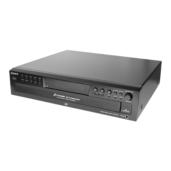
Sony CDP-CE275 Service Manual
Cd/sacd players & changers: carousel cd player 5 discs
Hide thumbs
Also See for CDP-CE275:
- Service manual (40 pages) ,
- Operating instructions manual (16 pages) ,
- Specifications (2 pages)
Advertisement
Quick Links
CDP-CE275/CE375
SERVICE MANUAL
Ver 1.1 2001.07
Compact disc player
Laser
Semiconductor laser (
Emission duration : continuous
Frequency response
2 Hz to 20 kHz
Dynamic range
More than 93 dB
Harmonic distortion
Less than 0.0045%
Outputs
Jack
type
ANALOG
Phono
OUT
jacks
DIGITAL
Optical
OUT
output
(OPTICAL)
connector
PHONES
Stereo
(CDP-CE375
phone
only)
jack
Sony Corporation
9-873-822-12
2001G0500-1
Home Audio Company
C 2001.7
Shinagawa Tec Service Manual Production Group
Photo: CDP-CE375
SPECIFICATIONS
= 780 nm)
0.5 dB
Maximum
Load
output level
impedance
2 V
Over 10
(at 50 kilohms) kilohms
–18 dBm
Wave
length:
660 nm
10 mW
32 ohms
Model Name Using Similar Mechanism
CD Mechanism Type
Base Unit Name
Optical Pick-up Name
General
Power requirements
120 V AC, 60 Hz
Power consumption
11 W
Dimensions (approx.)
430 x 110 x 400 mm
(w/h/d)
(17 x 4 3/8 x 15 3/4 in.)
incl. projecting parts
Mass (approx.)
5 kg (11 lbs 1 oz)
Supplied accessories
Audio cord (2 phono plugs – 2 phono plugs) (1)
Remote commander (remote) (1) (CDP-CE375 only)
R6 (size AA) batteries (2) (CDP-CE375 only)
Design and specifications are subject to change without notice.
COMPACT DISC PLAYER
US Model
Canadian Model
Australian Model
CDP-CE275/CE375
AEP Model
UK Model
E Model
CDP-CE375
CDP-CE345
CDM59-5BD27
BU-5BD27
PXR-104X
Advertisement

Summary of Contents for Sony CDP-CE275
- Page 1 (OPTICAL) connector PHONES Stereo 10 mW (CDP-CE375 phone only) jack Sony Corporation 9-873-822-12 2001G0500-1 Home Audio Company C 2001.7 Shinagawa Tec Service Manual Production Group Photo: CDP-CE375 Model Name Using Similar Mechanism CD Mechanism Type Base Unit Name Optical Pick-up Name...
-
Page 2: Section 4 Test Mode
CDP-CE275/CE375 Ver 1.1 2001.07 ADJ MODE NOTE: This mode cannot be performed without a general remote com- mander. 1. Chuck the CD first, and then turn OFF the power. 2. Short-circuit the test point TP1 (ADJ) of the MAIN board and ground with a lead wire. - Page 3 Buttons and Corresponding Button Numbers Button Button Number or Display DISC1 DISC2 DISC3 DISC4 DISC5 PLAY MODE PEAK SEARCH FADER REPEAT TIME H (PLAY) Partial lighting 1 X (PAUSE) Partial lighting 2 x (STOP) All lit EX-CHANGE DISC SKIP EDIT CHECK CLEAR AMS (push)
-
Page 4: Aging Mode
CDP-CE275/CE375 Ver 1.1 2001.07 AGING MODE For the aging mode, three modes of all mode, disc table mode, and loading mode are available. This set has the Aging mode for operation check of the mechanism deck. • If a failure occurred The aging operation stops and a faulty status is displayed on the fluorescent indicator tube. -
Page 5: Electrical Adjustments
Note: 1. CD Block is basically designed to operate without adjustment. There- fore, check each item in order given. 2. Use PATD-012 disc (4-225-203-01) unless otherwise indicated. 3. Use an oscilloscope with more than 10M 4. Clean the object lens by an applicator with neutral detergent when the signal level is low than specified value with the following checks. - Page 6 CDP-CE275/CE375 Ver 1.1 2001.07 E-F Balance Check Connection: oscilloscope BD board TP (TE1) TP (VC) – Procedure: Set the test disc (PATD-012). Disc chucking operation is [POWER] complete, then press the off. Connect an oscilloscpe to test point TP (TE1) and TP (VC) on the BD board.
- Page 7 SECTION 6 DIAGRAMS 6-1. NOTE FOR PRINTED WIRING BOARDS AND SCHEMATIC DIAGRAMS Note on Schematic Diagram: Note on Printed Wiring Board: • All capacitors are in µF unless otherwise noted. pF: µµF • X : parts extracted from the component side. 50 WV or less are not indicated except for electrolytics •...
- Page 8 6-3. SCHEMATIC DIAGRAM – BD Board – • See page 24 for Waveforms. (Page 21) • See page 24 for IC Block Diagrams. (RFAC) IC BD (RFDC) (TE1) (VC) (FE1) (SE1) IC BD The components identified by mark 0 or dotted line with mark 0 are critical for safety.
- Page 9 CDP-CE275/CE375 6-5. SCHEMATIC DIAGRAM – JUNCTION/SENSOR/LOADING MOTOR Boards – • See page 25 for IC Block Diagram. TO MAIN BOARD (Page 21) IC BD...
- Page 10 6-7. SCHEMATIC DIAGRAM – MAIN Board – • See page 24 for Waveform. (Page 19) (Page 23) (Page 17) CDP-CE275/CE375 The components identified by mark 0 or dotted Les composants identifiés par une marque 0 sont line with mark 0 are critical for safety. critiques pour la sécurité.
- Page 11 6-9. SCHEMATIC DIAGRAM – PANEL Section – (Page 21) (Page 21) The components identified by mark 0 or dotted Les composants identifiés par une marque 0 sont line with mark 0 are critical for safety. critiques pour la sécurité. Ne les remplacer que Replace only with part number specified.


